
PeakView RF IC electromagnetic field simulation software
PeakView RF IC electromagnetic field simulation software
Dedicated to the design and electromagnetic field simulation verification of radio frequency, microwave, millimeter wave and high-speed analog integrated circuits.
ABOUT software
PeakView is a 3D full-wave electromagnetic field simulation verification platform, dedicated to the design and electromagnetic field simulation verification of radio frequency, microwave, millimeter wave and high-speed analog integrated circuits. PeakView has built-in a rich library of passive components, including inductors, baluns, transmission lines, transformers, capacitors, T-coil, multilayer inductors, etc., which can be used for the synthesis and optimization of passive components, and can extract various types of passive components. The simulation accuracy of devices and interconnects meets the requirements of direct current (DC) to millimeter wave frequency bands and is widely used in the industry.
- Seamless integration with Cadence Virtuoso
- Seamless integration with Cadence and Mentor's layout parasitic parameter extraction tools
- Compatible with Synopsys' flagship emulator Hspice
- Support one-click conversion of ITF/IRCX/ICT format process files to generate profile files containing media layer, metal and substrate information and layer mapping information

The main function
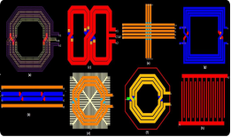
Pcircuit passive component library
The EMD module has a built-in parameterized passive component model library Pcircuit. The software can synthesize and optimize passive components. At the same time, it can set PGS, guard ring, slow wave structures, and the drc rule has been set in the profile, which can ensure the comprehensive generation of EMD The devices meet the DRC design rules.
The model is written in Python and can be customized based on customer needs.
The types of passive components include but are not limited to the following types:
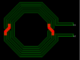
- Inductor: Including square inductance, circular inductance, octagonal inductance, low-side capacitance inductance, figure eight inductance, etc.;
- Transformer (Transformer): Supports 1:1, 1:N transformers to meet the user's design in areas such as DC isolation, impedance changes, and differential inductance;
- Balun: supports multi-shape balun topology; supports symmetrical and asymmetrical design of ports to meet layout requirements; supports individual adjustment of physical parameters of primary and secondary solenoids to improve design flexibility; supports stacked structure to optimize layout area ;
- Transmission Line: Including but not limited to microstrip line, strip line, CPW; supporting single-ended and differential CPW design analysis; supporting multi-layer penetration of coplanar ground, and shielding layer setting; providing various curve formulas of transmission line , Including characteristic impedance, differential impedance, return loss, insertion loss, absolute loss (Gmax), differential line phase error formula, etc.
- Interconnect: Provide any interconnection, differential crossover, multi-layer crossover and other topological structures to assist users in the performance impact analysis of complex layout structures.
- T-coil: Provides symmetric T-coil and asymmetric T-coil topological structures to facilitate the design of different application scenarios; provides high-level topological structures such as port symmetry, stacking, and symmetric stacking; supports comprehensive optimization of T-coil multiple indicators, Including L1, L2, coupling coefficient, bridge capacitance index, etc.; provide flow description of T-coil simulation design.
- Multi-layer stacked inductor MLS; supports multi-layer parallel, series, strong parallel and weak parallel forms;
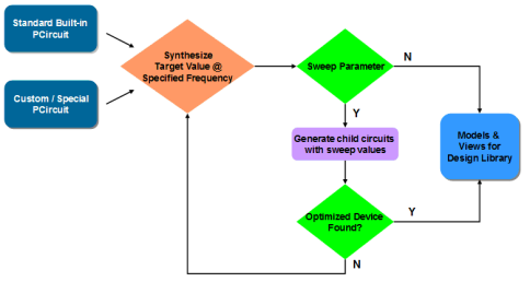
Synthesis and optimization of passive components
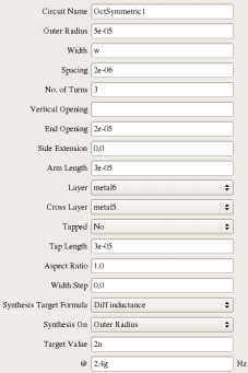
- Comprehensive function: take the software built-in function (Ld, L, Qd, R, etc) as the target value or user-built function as the target for synthesis, and the software automatically calculates the device that meets the target requirements;
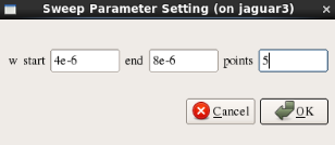
- Scanning function: allows users to scan multiple layout parameters at the same time (such as inductance width, outer diameter, number of turns, etc.); as long as they are defined in the device library, they can be scanned as scanning targets;
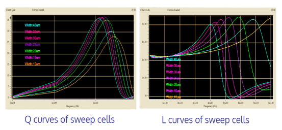
- Synthesis + Scan: Use synthesis and scanning together to design the optimal device; the user sets a comprehensive target value and sets multiple variables for scanning at the same time, and the software synthesizes multiple sizes that meet the target value within the set parameter range Device, for users to choose the best device (higher Q value or smaller area) among these devices that meet the requirements, saving costs and improving design quality;
LEM electromagnetic field simulation
Three-dimensional electromagnetic simulation based on Virtuoso/Laker/GDS layout layout environment or general layout files, which can be used to check circuit connections, analyze current and voltage distribution, and electromagnetically perform any shape layout (path, arbitrary polygon, metal filling, slotting, etc.) Simulation, generate S parameter model, RLCK circuit physical model, symbol, spice, etc. The result can be synchronized to Cadence, and combined circuit simulation with Spectre/SPICE circuit simulator.
- Different simulation types can be set for different metal layers, which saves simulation time and improves simulation accuracy;
- With full consideration of the skin effect, the thick metal can be divided into three different directions of nu, nv, and nz more finely to improve the simulation accuracy, support the current division of multiple layers, and improve the simulation accuracy;
- Post-processing function, data processing can be carried out conveniently;
- Support temperature and corner scanning, which can scan certain temperature points or corners alone, or a combination of temperature and corner scanning;
- Support super-cell function, you can substitute Layout into schematic for simulation to fully verify device performance;
- The simulation results consider the layout effect (LDE): Peakview will recognize the LDE information in the PDK, and map the LDE information with the sheet resistance change table and the line width change table when converting the configuration file. During simulation, peakview looks up the table according to different design dimensions, and calls the actual sheet resistance and line width values to ensure that the simulation results are closer to the measured values.
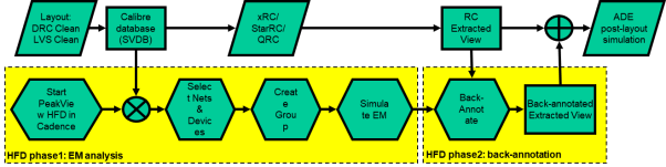
HFD module-fully automated high-frequency parasitic L extraction and simulation
In the design of high-frequency integrated circuits, traditional Calibre can only extract RC, but cannot accurately extract parasitic L. HFD can extract parasitic parameters accurately for critical paths and passive components, generate complete RLCK or full-wave parameter models, automatically extract layouts and extract parasitics Parameters, perform simulation, automatically replace back annotation with RC extract view, and perform joint circuit simulation with Spectre/Spice circuit simulator.
- You don’t need to cut out the picture manually, just click the mouse directly;
- You can click on the schematic or click on the layout;
- Only need to go through lvs once, the process is simple;
- Automatic counter-marking, confirm the corresponding relationship through CCI data, accurate and convenient;
